What is a CMOS sensor?
What is a CMOS sensor?
A CMOS sensor is an electronic chip that converts photons to electrons for digital processing. The chip is based on complementary metal oxide semiconductor (CMOS) technology, which is widely used for many of today’s integrated circuits. CMOS itself is a type of metal-oxide semiconductor field-effect transistor (MOSFET), a common type of field-effect transistor that can act as an electrical switch or amplifier.
CMOS sensors are used to capture images in digital cameras, digital video cameras and digital CCTV cameras. They can also be found in devices, such as scanners, barcode readers and astronomical telescopes. In addition, they’re used for robotic vision, optical character recognition (OCR), satellite photography and radar imaging enhancement, especially for meteorology. CMOS sensors are also found in internet of things (IoT) devices. These sensors enable IoT devices to respond to image input from the physical environment.
How do CMOS sensors work?
A CMOS sensor contains an array of minuscule cells (photodiodes) that capture photons at their various wavelengths and intensity when the light strikes the chip’s surface. A lens is often used to focus the light before it reaches the sensor, as is the case of digital cameras. The CMOS sensor is typically covered by a mosaic array of red, blue and green filters that the chip uses for color detection.
The photodiodes convert the captured photons into electrons, much like tiny solar cells. Each photodiode is surrounded by transistors that amplify the electron charges and transmit them across the chip via tiny wires in the circuitry. The transistors also reset the photodiodes so they’re ready for the next image.
In addition to the sensor itself, a single CMOS chip can incorporate other functions, which eliminates the need to offload those functions to another device. This can help improve read-out times and reduce power consumption, compared to other types of image sensors.
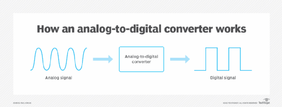
One of the chip’s most important features, outside of the photodiodes, is the analog-to-digital converter, which is built directly into the circuit. It reads the electron charges collected by the photodiodes and translates them into binary data that is then used to create the digital image. A CMOS sensor typically incorporates other functionalities as well, such as image processing, exposure control or temporary buffering.

The process of manufacturing CMOS sensors is similar to the process used to build other types of CMOS chips, such as those used for microprocessors or memory modules. CMOS sensors can be built in the same high-volume wafer plants as the other chips, often leveraging similar methods.
For example, the manufacturing process commonly incorporates photolithography, a production method that uses light to transfer a circuit’s pattern to a thin photosensitive layer covering the silicon substrate. This pattern is then transferred to the substrate through a multiphase etching process.
CMOS sensors vs. CCD sensors
CMOS sensors are often compared to charge-coupled device (CCD) sensors, especially when discussing digital cameras. CCD sensors have a similar structure to CMOS sensors, but they take a different approach to how they shift electrons off the sensor. These differences result in each type offering both advantages and disadvantages when compared.
CMOS sensors are generally easier to build than CCD sensors. Manufacturers can take advantage of the same processes and infrastructure used to build other types of chips, making it possible to create CMOS sensors at a larger scale and lower cost. CCD sensors have more complex circuitry, which translates to a more complex manufacturing process. As a result, CCD sensors are more expensive to build, limiting their use in low-cost consumer devices.
CMOS sensors are also faster than their CCD counterparts because CMOS chips can incorporate functionality directly into the chip. In addition to capturing photons, they can carry out other operations important to creating quality images. Because of this multifunction design, the electrical charges can be read more easily and quickly, resulting in faster readout times.
The CMOS architecture also reduces the amount of power needed to capture an image. In contrast to CMOS sensors, CCD sensors must actively use power to gather light because the cells are not surrounded by transistors, causing them to be less power-efficient.

At the same time, the CCD architecture also offers several benefits over CMOS. CCD sensors have long been known for producing less noise, achieving greater light sensitivity and delivering higher image quality. That said, advances in CMOS technology have greatly improved CMOS sensors, and the distinction in quality between the two types is no longer as clear-cut as it once was.
For example, Canon has developed a CMOS sensor that locates the photodiodes above the transistor layer, making light collection more efficient. The result is less image noise and better image quality. Such improvements are putting CMOS sensors on par with CCD and helping them make inroads into the higher-end digital camera market and in other areas.
The key to making effective use of IoT devices is to make sure to start an IoT strategy on the right foot and to understand how the edge and IoT are intertwined with one another.